Soitec Products and Services
1 /8Pages

Soitec Products and Services
1 /8Pages
Catalog excerpts
Soitec Products and Services Semiconductor Materials & Equipment - Solar Energy - Lighting
Open the catalog to page 1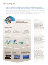
The Company Soitec is a world leader in designing and manufacturing high-performance semiconductor materials, using its unique expertise to serve the electronics, solar energy and lighting markets. Since its creation in 1992, Soitec has continued to grow by cultivating innovation and focusing on developing differentiating technologies that add maximum value to end products. As an industrial company, Soitec has built its reputation on developing and manufacturing its flagship material, SOI (silicon-on-insulator), which is based on the revolutionary Smart Cut™ “atomic scalpel” technology. High-Performance...
Open the catalog to page 2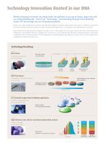
Technology Innovation Rooted in our DNA Market-changing innovation has always been the pathway to success at Soitec, beginning with our initial breakthrough – Smart Cut™ technology – and extending through Smart Stacking™, Soitec CPV technology and our full product portfolio. Soitec has nearly 3,000 active patents and files 350 additional patent applications each year. In addition to patents for which we hold sole ownership, we also license technologies from our research and development partners. Our research and development program focuses on four major goals: continuing to reduce the size of...
Open the catalog to page 3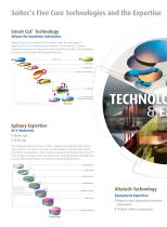
Soitec’s Five Core Technologies and the Expertise Smart Cut™ Technology Silicon-On-Insulator Substrates Soitec’s silicon-on-insulator (SOI) wafers cover the full range of applications for microelectronics markets. Our Smart Cut™ wafermanufacturing technology gives us the flexibility to tailor SOI substrates to meet the most demanding specifications. 1_Initial silicon 2_Oxidation 3_Implantation 4_Cleaning and bonding 6_Annealing and CMP touch polishing 7_Donor wafer becomes new wafer A Epitaxy Expertise III-V Materials GaAs epi GaN epi For epitaxial GaAs structures, Soitec materials are tailored...
Open the catalog to page 4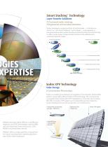
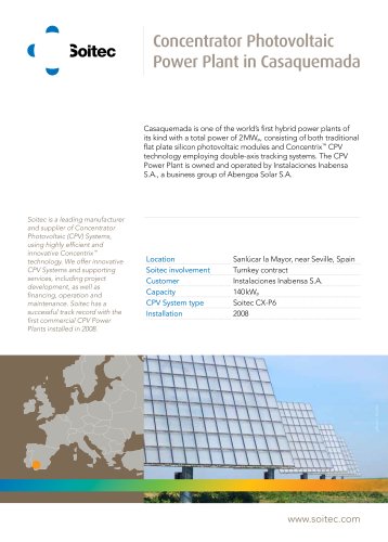
Smart Stacking™ Technology Layer-Transfer Solutions Processed wafer stacking Engineered and bonded substrates Soitec leverages a unique portfolio of technologies — including our Smart Cut™ and Smart Stacking™ technologies — and expertise in low-temperature direct wafer bonding and mechanical-chemical thinning to offer a wide range of layer-transfer solutions that address each customer’s specific needs. Initial processed wafer Initial bulk or processed wafer Final wafer after Smart Stacking™ Soitec CPV Technology Solar Energy Concentrator Photovoltaic Soitec is a leading manufacturer and supplier...
Open the catalog to page 5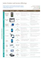
Soitec Product and Service Offerings Soitec’s products and technologies dramatically improve energy efficiency, performance, miniaturization, reliability and the quality of daily life. Typical Applications Typical Markets Soitec Products Lines Specifications SOI wafer diameters: 200 mm and /or 300 mm Ultra-thin silicon-on-insulator with: Digital CMOS: Planar Fully Depleted (FD-SOI) • Top silicon: 10 nm to 30 nm • Buried oxide layer: 10 nm to 145 nm • Uniformity: ±5 Å min. – max. range (all points, all wafers) Silicon-on-insulator with: Digital CMOS: FinFET • Top silicon: 20 nm to 100 nm • Buried...
Open the catalog to page 6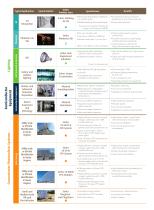
Typical Applications Typical Markets Soitec Products Lines Specifications Specifications • Direct bonding based on dielectric or metallic layers • Innovative solutions to improve performance, form factor and cost • Multiple stacking of processed layers • Customized solutions Products also available: Stacking for Imager and Stacking for MEMS Silicon-on-insulator with: • Top silicon: 200 nm to 2000 nm • Thick buried oxide for optical confinement • Excellent top-silicon crystal quality enabling low-loss waveguide Soitec GaN Engineered Substrate • Buried oxide layer: 1 µm to 3 µm • Good thickness...
Open the catalog to page 7
Worldwide Contacts Semiconductor Materials Solar Energy Global presence Altatech Equipment Smart Cut™, Smart Stacking™ , Smart Cell™ , Premium SOI™, Wave SOI™, eSI™, Smart Power SOI™, Imager SOI™, Plug & Sun™ and Soitec™ are trademarks of Soitec S.A. © 2014 Soitec S.A. | Version: June 2014, design: VHOX.com Cover photos: Christian Morel, Tony Tremblay (iStock), Soitec, Apomares (iStock). Soitec S.A. and its subsidiaries or affiliates, officers, employees, representatives do not warrant the accuracy or completeness of the information, text, graphics other items contained inside this leaflet. ©...
Open the catalog to page 8All Soitec catalogs and technical brochures
 Puertollano
2 Pages
 Casaquemada
2 Pages
 products_services
7 Pages
 Soitec Plug&Sun
2 Pages