products_services

products_services
Soitec is a global leader in semiconductor materials, focusing on innovation and technology development to enhance energy and electronics products. Established in 1992, the company is renowned for its Silicon-on-Insulator (SOI) materials and Smart Cut™ technology. Soitec also leads in concentrator photovoltaic (CPV) systems with its Concentrix™ technology, catering to markets like mobile electronics, computing, automotive electronics, and lighting.
Soitec has a global manufacturing capacity of 2 million wafers per year for electronics and 350 MW per year for solar energy. The company emphasizes green electronics, energy, and lighting, with a strong focus on performance and energy efficiency.
Innovation is central to Soitec's success, with technologies like Smart Cut™, Smart Stacking™, and Concentrix™. The company holds nearly 3,000 active patents and files 350 new applications annually. R&D focuses on transistor miniaturization, adding new circuit functions, III-V materials engineering, and high-efficiency solar cells.
Soitec's roadmap includes More Moore (transistor miniaturization), More than Moore (enhanced circuit features), III-V materials for lighting and power electronics, and high-efficiency solar cells for CPV systems.
Soitec's core technologies include Smart Cut™ for SOI substrates, Smart Stacking™ for layer-transfer solutions, epitaxy expertise for III-V materials, and Altatech technology for materials deposition and defect inspection.
Soitec offers products that improve energy efficiency, performance, and reliability across various applications and markets. Key product lines include digital CMOS, RF on SOI, power and analog on SOI, image sensors, MEMS, photonics, 3D integration, and LED substrates.
Soitec provides utility-scale CPV power plants and off-grid solutions like Plug & Sun™, emphasizing high efficiency, low cost, and local job creation.
Soitec operates globally with offices in Europe, America, Asia, and Africa, providing comprehensive support and services across its semiconductor and solar energy sectors.
Catalog excerpts
Soitec Products and Services Semiconductor Materials & Equipment – Solar Energy
Open the catalog to page 1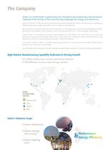
The Company Soitec is a world leader in generating and manufacturing revolutionary semiconductor materials at the frontier of the most exciting challenges for energy and electronics. Since its creation in 1992, Soitec has continued to grow by cultivating innovation and focusing on developing differentiating technologies that add maximum value to end products. As an industrial company, Soitec has built its reputation on developing and manufacturing its flagship material, SOI (Silicon-on-Insulator), which is based on the revolutionary Smart Cut™ “atomic scalpel” technology. Today Soitec is developing...
Open the catalog to page 2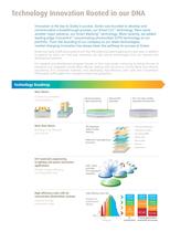
Technology Innovation Rooted in our DNA Innovation is the key to Soitec’s success. Soitec was founded to develop and commercialize a breakthrough process, our Smart Cut™ technology. Next came another major advance, our Smart Stacking™ technology. More recently, we added leading-edge Concentrix™ concentrating photovoltaic (CPV) technology to our portfolio. From the founding of our company to our latest technologies, market-changing innovation has always been the pathway to success at Soitec. Soitec has nearly 3,000 active patents and files 350 additional patent applications each year. In addition...
Open the catalog to page 3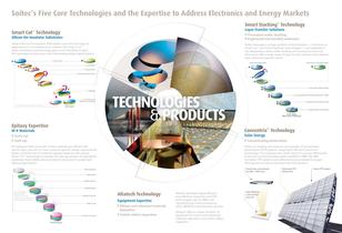
Soitec's Five Core Technologies and the Expertise to Address Electronics and Energy Markets Silicon-On-lnsulator Substrates Soitec's Silicon-On-lnsulator (SOI) wafers cover the full range of applications for microelectronics markets. Our Smart Cut™ wafer-manufacturing technology gives us the flexibility to tailor SOI substrates to meet your most demanding design specifications 7_Donor wafer becomes new wafer A Epitaxy Expertise lll-V Materials For epitaxial GaAs structures, Soitec materials are tailored with atomic-layer precision to meet customer-specific design requirements Soitec combines...
Open the catalog to page 4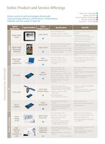
Soitec Product and Service Offerings Soitec's products and technologies dramatically improve energy efficiency, performance, miniaturization, reliability and the quality of daily life. Smart Stacking ™ technology < Digital CMOS: Digital CMOS: Planar Fully Digital CMOS: Typical Markets „ j*°!?ef • Silicon-On-lnsulator with: • Buried oxide layer: 50 nm standard Ultra-thin Silicon-On-lnsulator with: • Buried oxide layer: 10nmto 145nm Silicon-On-lnsulator with: • Buried oxide layer: 50 nm Fin height and isolation built into • Faster and easier process • Optimized cost of ownership • Excellent electrical...
Open the catalog to page 5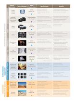
Specifications Benefits Photonics on SOI Soitec MEMS SOI Soitec Stacking for MEMS Soitec Photonics SOI • Faster learning and ramp-up • Top silicon: 1.5 µm min. • Higher yields in volume production • Buried oxide layer: 145 nm to 500 nm • Lower total cost of ownership • Direct-bonding and thinning techniques on processed SOI and bulk wafers • Low-stress bonding compatible with color filter arrays for any pixel sizes • Proven reliability in extreme environments Silicon-On-Insulator with: • Excellent uniformity Top silicon and buried oxide layer thickness adaptable to any customer application •...
Open the catalog to page 6
Soitec (headquarters) Parc Technologique des Fontaines 38190 Bernin (France) T. +33 (0)4 76 92 75 00 F. +33 (0)4 38 92 71 89 www.soitec.com Worldwide Contacts Semiconductor Materials Solar Energy Europe Europe Soitec (headquarters) Parc Technologique des Fontaines 38190 Bernin (France) T. +33 (0)4 76 92 75 00 | F. +33 (0)4 38 92 71 89 Soitec Solar 54 avenue Marceau 75008 Paris (France) T. +33 (0)1 47 23 90 65 | F. +33 (0)1 47 23 90 99 Soitec Paris Sud Place Marcel Rebuffat Parc de Villejust 91971 Courtabœuf (France) T. +33 (0)1 69 31 61 30 Soitec Solar GmbH Boetzinger Strasse 31 79111 Freiburg...
Open the catalog to page 7All Soitec catalogs and technical brochures
 Soitec Products and Services
8 Pages
 Puertollano
2 Pages
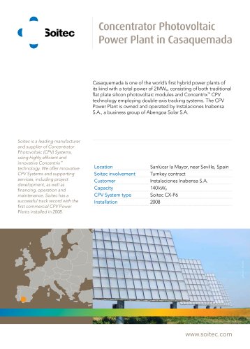 Casaquemada
2 Pages
 Soitec Plug&Sun
2 Pages